AR
C
HIVE INF
O
RMATI
O
N
ARCHIVE INFORMATION
MRFG35010R1
3
RF Device Data
Freescale Semiconductor
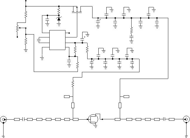
Figure 1. 3.4 - 3.6 GHz Single Supply Bias Sequencing Test Circuit Schematic
D1
C11
R3
R2
R1
C12
R7
C10
C9
C13 C15 C18
C14 C16 C19
R6
R4
R8
C1
Z1
C21
Q1
C7 C5 C3
C8 C6 C4 C2
U1
NC
RF
INPUT
RF
OUTPUT
VDD
C17
R9
C20
1
2
3
4
8
7
6
5
C1, C21 6.8 pF Chip Capacitors, ATC
C2, C20 10 pF Chip Capacitors, ATC
C3, C19 100 pF Chip Capacitors, ATC
C4, C18 100 pF Chip Capacitors, ATC
C5, C10, C16, C17 1000 pF Chip Capacitors, ATC
C6, C11, C12, C15 0.1 μF Chip Capacitors, ATC
C7, C14 39K Chip Capacitors, ATC
C8, C13 22 μF Tantalum Chip Capacitors
C9 6.8 μF Tantalum Chip Capacitor
D1 5.1 V Zener Diode, MA8051CT-ND
R1 22.1 kΩ,
1/4 W 1%, Chip Resistor
R2 5K Trim Pot, #3224W-1-502E
R3 12 kΩ,
1/4 W 1%, Chip Resistor
R4 100 kΩ,
1/4 W 1%, Chip Resistor
R5 39 kΩ,
1/4 W 1%, Chip Resistor
R6 10 Ω,
1/4 W 1%, Chip Resistor
R7 2.2 kΩ,
1/4 W 1%, Chip Resistor
R8, R9 50 Ω,
1/4 W 1%, Chip Resistors
U1 Voltage Converter, LTC 1261
Q1 Switch, MTP23P06V
PCB Rogers RO4350, 0.020″, εr
= 3.50
Z1 0.044″
x 0.250
″
Microstrip
Z2 0.044″
x 0.030
″
Microstrip
Z3 0.615″
x 0.050
″
Microstrip
Z4 0.044″
x 0.070
″
Microstrip
Z5 0.270″
x 0.490
″
Microstrip
Z6 0.044″
x 0.470
″
Microstrip
Z7 0.434″
x 0.110
″
Microstrip
Z8, Z11 0.015″
x 0.527
″
Microstrip
Z9, Z10 0.290″
x 90
°
Microstrip Radial Stub
Z12 0.184″
x 0.390
″
Microstrip
Z13 0.040″
x 0.580
″
Microstrip
Z14 0.109″
x 0.099
″
Microstrip
Z15 0.030″
x 0.225
″
Microstrip
Z16 0.080″
x 0.240
″
Microstrip
Z17 0.044″
x 0.143
″
Microstrip
R5
Z2
Z3
Z4
Z5
Z6
Z7
Z12
Z13
Z14
Z15
Z16
Z17
Z9 Z10
Z8 Z11


发布紧急采购,3分钟左右您将得到回复。
相关PDF资料
MRFG35020AR1
TRANSISTOR RF 20W GAAS NI-360
MRFG35030R5
MOSFET RF 3550MHZ 30W 12V HF-600
MSD6100RLRAG
DIODE SW DUAL CC 100V TO-92
MSQC4911C
LED 7-SEG CLOCK 4DIG CA HRED .4"
MSRD620CTG
DIODE ULT FAST 200V 3A DPAK
MSRD620CTRG
DIODE ULTRA FAST 200V 3A DPAK
MTGEZW-00-0000-0N00J040H
XLAMP MTG SERIES LED WHITE
MUR1020CTPBF
DIODE ULT FAST 200V 5A TO220AB
相关代理商/技术参数
MRFG35010R5
功能描述:TRANSISTOR RF FET 3.5GHZ NI360HF RoHS:是 类别:分离式半导体产品 >> RF FET 系列:- 产品目录绘图:MOSFET SOT-23-3 Pkg 标准包装:3,000 系列:- 晶体管类型:N 通道 JFET 频率:- 增益:- 电压 - 测试:- 额定电流:30mA 噪音数据:- 电流 - 测试:- 功率 - 输出:- 电压 - 额定:25V 封装/外壳:TO-236-3,SC-59,SOT-23-3 供应商设备封装:SOT-23-3(TO-236) 包装:带卷 (TR) 产品目录页面:1558 (CN2011-ZH PDF) 其它名称:MMBFJ309LT1GOSMMBFJ309LT1GOS-NDMMBFJ309LT1GOSTR
MRFG35020AR1
功能描述:射频MOSFET电源晶体管 3.5GHZ 20W GAAS NI360 SH RoHS:否 制造商:Freescale Semiconductor 配置:Single 晶体管极性: 频率:1800 MHz to 2000 MHz 增益:27 dB 输出功率:100 W 汲极/源极击穿电压: 漏极连续电流: 闸/源击穿电压: 最大工作温度: 封装 / 箱体:NI-780-4 封装:Tray
MRFG35020AR5
功能描述:射频GaAs晶体管 3.5GHZ 20W GAAS NI360 SH RoHS:否 制造商:TriQuint Semiconductor 技术类型:pHEMT 频率:500 MHz to 3 GHz 增益:10 dB 噪声系数: 正向跨导 gFS(最大值/最小值):4 S 漏源电压 VDS: 闸/源击穿电压:- 8 V 漏极连续电流:3 A 最大工作温度:+ 150 C 功率耗散:10 W 安装风格: 封装 / 箱体:
MRFG35030R5
功能描述:MOSFET RF 3550MHZ 30W 12V HF-600 RoHS:是 类别:分离式半导体产品 >> RF FET 系列:- 产品目录绘图:MOSFET SOT-23-3 Pkg 标准包装:3,000 系列:- 晶体管类型:N 通道 JFET 频率:- 增益:- 电压 - 测试:- 额定电流:30mA 噪音数据:- 电流 - 测试:- 功率 - 输出:- 电压 - 额定:25V 封装/外壳:TO-236-3,SC-59,SOT-23-3 供应商设备封装:SOT-23-3(TO-236) 包装:带卷 (TR) 产品目录页面:1558 (CN2011-ZH PDF) 其它名称:MMBFJ309LT1GOSMMBFJ309LT1GOS-NDMMBFJ309LT1GOSTR
MRFIC0001
制造商:MOTOROLA 制造商全称:Motorola, Inc 功能描述:QUADRATURE MODULATOR INTEGRATED CIRCUIT
MRFIC0903
制造商:MOTOROLA 制造商全称:Motorola, Inc 功能描述:ANTENNA SWITCH GaAs MONOLITHIC INTEGRATED CIRCUIT
MRFIC0904
制造商:MOTOROLA 制造商全称:Motorola, Inc 功能描述:900 MHz GaAs TWO STAGE DRIVER AMP INTEGRATED CIRCUIT
MRFIC0912
制造商:MOTOROLA 制造商全称:Motorola, Inc 功能描述:900 MHz GaAs INTEGRATED POWER AMPLIFIER
